Copyright 2014 CVInc all rights
info@covinc.com
CVI Technology
CVI bumps single die, partial and
complete wafers to reflect true flip chip die.
UBM is added followed by solder
and reflow.
No gold stud bump and epoxy
mess!
Prototype packaging is essential in the
prototype and development phases
where long lead times can be project
killers.
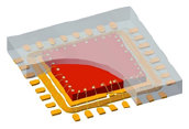
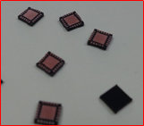
To better simulate real world CVI offers
overmolded QFN and modular
packages.
Our expanded capability includes higher
density leads as well as new
integrated coiled packaging.
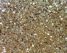
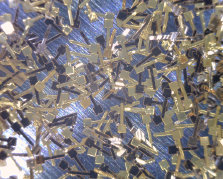
PCB repair kits.
Lead, pads, and pads
with traces.
Various sizes and shapes.
Pads as small as 60um


